
Infineon Technologies (IFX GY): Power Overwhelming
A look at the power semis bottleneck and how Infineon might benefit

Welcome to Bristlemoon Capital! We have written previously on AERO SW, AER, ADBE, TDG, the AI bubble, FICO, GOOGL, ASML, SNPS, UNH, META, GRND, HEM SS, MELI, U, APP, PDD, IBKR, PAR, AER, PINS, BROS, MTCH, CPRT, RH, EYE, and TTD.
If you haven’t subscribed, you can join 6,125 others who enjoy our deep dives and investment insights here:
Australian wholesale investors looking to invest in the Bristlemoon Global Fund can do so via this link.
Table of Contents
Introduction to the business and recent financial performance
The power conversion challenge for AI data centers
The legacy architecture and its limits
Two converging architecture standards
The 800V power delivery chain: from grid to transistor
The AI data center opportunity for Infineon
Stage by stage
Sizing the AI data center opportunity
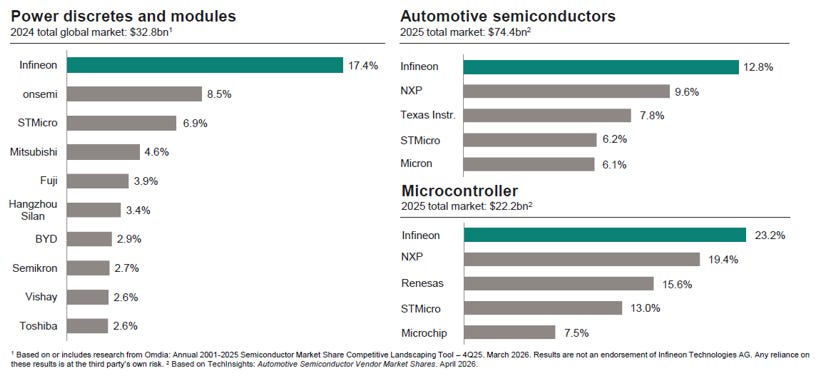
Competition and market share
Automotive: the bull case that never was
The bull case that never was
Should we be excited about an automotive recovery?
Green Industrial Power: the forgotten segment
The solid state transformer opportunity
Is there an emerging MCU shortage?
Introduction
Infineon Technologies is not a stock that generates much excitement at dinner parties – nor at AI investor parties, it would seem – until recently. The Munich-headquartered diversified power semiconductor company lacks the headline profile of Nvidia, the Uber driver name recognition of Micron and SK Hynix, or the obscene torque of the optical bottleneck stocks. For most of the post-GFC cycle, Infineon occupied a corner of the market that can be loosely described as “European industrial cyclical with some EV exposure”, and the company’s stock price largely reflected this. Indeed, the last time we seriously looked at the company, it was coming off the back of the post-COVID automotive/industrial shortage and preparing for the global high voltage EV boom that never materialized. The stock spent most of the past four years treading water, before doubling in the space of ~8 weeks.
What has changed over the past twelve months is that the center of gravity for semiconductor demand fractured away from compute (GPUs and ASICs – too boring) and shifted across the supply chain into higher-beta areas such as memory, optical networking and packaging. The latest area to capture the attention (and imagination) of the market is power conversion and management within AI data centers. The AI DC buildout has surfaced a constraint that was obvious in retrospect: raw compute power is now scaling faster than the electrical infrastructure that delivers energy to it. Here, we refer specifically to the power infrastructure from the boundary of the DC facility to the point-of-load (POL) on the GPU itself.
Solving that constraint requires a complete architectural overhaul of data center power delivery, from the traditional 480VAC → 12VDC to 800V high voltage DC (HVDC) led by Nvidia’s 800VDC reference design and the +/- 400VDC Mt Diablo architecture developed by the hyperscalers. Regardless of which design becomes standard, the overhaul depends heavily on the wide-bandgap semiconductors, power MOSFETs and voltage regulator modules that form the core of Infineon’s product portfolio.
While the 800VDC architecture was unveiled last year, it was only in the last couple of months where it felt like everyone was talking about data center power and power semis as the next optical or memory play. The result: IFX and its power semis peers have rerated vertically since the end of March as this narrative gathered steam. Unlike some of the more speculative AI narrative pumps, we’d say this rerating is not without merit. Infineon reported Q2 FY2026 results that beat expectations, raised its full-year sales and margin guidance, confirmed its AI revenue targets for FY2026 and FY2027, and announced the early opening of its Dresden Smart Power Fab Module 4 to serve overwhelming AI power demand.
Furthermore, the 800VDC transition strikes us as a cycle that has legs. Unlike AI servers or memory where a double-digit sales growth trajectory next year could spell disaster for the relevant stocks, the 800VDC architecture is a quasi zero-to-one transition. That is to say, even if Nvidia’s Rubin and Rubin Ultra server generations sell like cold scones, the transition to 800VDC must happen as current data center power architecture simply cannot handle the power density of future AI racks.
In this piece we examine Infineon’s four main investment angles: overwhelmingly dominated by AI data centers today, but encompassing also a potential automotive recovery, industrial power and electrification, and an industry-leading microcontroller business. Ultimately, while we like Infineon as a business, the violence with which this sleepy power/analog stock has rerated to all-time highs (on both price and multiple) has likely pulled forward substantial future returns and leaves us lukewarm on IFX as an investment.
Business overview
Infineon was spun out of Siemens in 1999 and has grown from a diversified industrial semiconductor company into a more focused power and embedded systems specialist through a series of transformative acquisitions: International Rectifier in 2015 ($3 billion), Cypress Semiconductor in 2020 ($9.4 billion), and most recently the Marvell automotive Ethernet business for $2.5 billion in FY2025.
The company’s competitive position rests on three pillars. First, it is the global leader in power semiconductors across silicon MOSFETs, IGBTs, and silicon carbide (SiC) MOSFETs – devices that control and convert electricity in everything from server power supplies to electric vehicle traction inverters. Second, it holds the #1 position in microcontrollers (MCUs) globally, with approximately 23.2% market share by revenue through its AURIX product family. Third, it occupies leading positions in several niche but strategically important markets including automotive radar sensors, smart card security controllers, and industrial motor drive power modules.
Source: Infineon
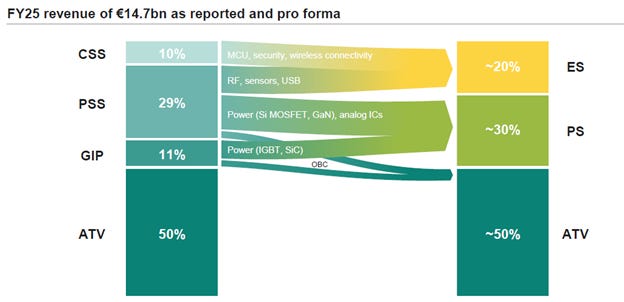
Through FQ2 FY2026 (March 2026 quarter), Infineon reported four segments:
Automotive (ATV) at 50% of FY25 of revenue covers power semiconductors and MCUs for passenger and commercial vehicles;
Power & Sensor Systems (PSS) at 29% spans power semiconductors for servers, consumer electronics, and mobile devices, plus automotive radar sensors;
Green Industrial Power (GIP) at 11% covers power components for industrial motor drives, HVAC systems, solar inverters, and grid infrastructure; and
Connected Secure Systems (CSS) at 10% covers smart cards, security controllers, and IoT connectivity.
Effective July 1, 2026, Infineon will reorganize into three divisions: Automotive (~50% of revenue), Power Systems (~30%), and Edge Systems (~20%). The restructuring consolidates AI data center and industrial power exposure into a single Power Systems reporting unit rather than split across two segments, making the AI opportunity more visible to investors.
Source: Infineon
Recent financial performance
Q2 FY2026 results came in ahead of expectations on the critical metrics, indicating the protracted cyclical trough is firmly in the rearview mirror. Indeed, management’s confident tone on the Q2 call marks a stark contrast to the cautious language that was still being used as recently as January 2026.
“A broader upswing across many end markets is clearly on the horizon. We are seeing rising demand in several key markets. While geopolitical conflicts continue to weigh on people and markets, our business indicators such as order intake, delivery times, cancellation rates, and inventory levels are showing a significantly improved picture. […] The market development in industrial applications is being supported by rising demand for energy infrastructure. In the automotive sector, order intake is rising as customers begin to replenish their low inventory levels. However, electromobility remains in difficult waters, while we are seeing a positive global trend in software-defined vehicles. Overall, demand in our end markets is improving significantly. We are preparing for a broad-based upswing.” – CEO, Q2 FY2026 analyst call
Compared to a quarter ago:
“Near-term indicators such as order intake or lead times are now starting to align in a positive way, and visibility is improving. That said, we feel our view of a gradual and uneven recovery remains appropriate for the time being. […] Automotive and industrial markets are beyond the cyclical trough, but demand has yet to really inflect. Consumer, compute ex-AI, and communication markets are in the early innings of the upcycle. AI remains the clear standout, continuing its extraordinary growth propelled by sustained massive investment in data centers and related infrastructure.” – CEO, Q1 FY2026
Revenue was €3.8 billion, up 4% QoQ and 6% YoY, with a segment result margin of 17.1%. The positive surprise was driven by stronger-than-expected AI power demand and a meaningful recovery in the GIP segment (+15% QoQ). Infineon raised its full-year FY2026 revenue guidance to above €16 billion with a segment result margin of approximately 20%, a step up from the high-teens margin guided earlier in the fiscal year and an upgrade to sellside consensus. The company simultaneously confirmed its dedicated AI power revenue targets of €1.5 billion in FY2026 and €2.5 billion in FY2027. The AI business is, per management’s own characterization, in allocation through FY2026 as demand exceeds available supply.
“Currently, our AI business is in allocation and we are converting capacities from other areas as well as ramping new ones as quickly as possible. Given the unabated momentum, we are reconfirming our guidance of dedicated AI power revenues of EUR1.5 billion for ‘26 as well as our indication of EUR2.5 billion for ‘27, irrespective of a weaker US dollar.” – CEO, Q2 FY2026 analyst call
“As we said carefully in our prepared script, the longer the allocation lasts on AI and adjacent markets, the more positive dynamic for pricing could be also visible still in the remaining quarters.” – CFO, Q2 FY2026 analyst call
The most significant near-term operational event is therefore the opening of Dresden Smart Power Fab Module 4 on July 2, 2026, earlier than the originally planned autumn timeline. Dresden Module 4 represents Infineon’s largest single investment at approximately €5 billion and is the primary production site for AI silicon MOSFETs. Its ramp through H2 FY2026 and into FY2027 is the central production lever underpinning management’s €2.5 billion FY2027 AI revenue target. The company is also converting underutilized silicon IGBT capacity (for EV and PV inverters) into AI silicon MOSFETs and further expanding power-related analog and sensor capacity by pulling forward an additional €500 million of capex.
“And for the time being, as I mentioned also in my summary, we are less hopeful for the XEV market. In fact, we believe that the development will be showing less growth than many market participants anticipate. And in the IGBT domain, for XEV as much as for certain applications in photovoltaics, we believe that it’s better to use this capacity, as I outlined in my intro, to convert it to leading-edge silicon MOSFETs and use it for the fast-growing, margin-accretive AI business.” – CEO, FY2025 analyst call
“These investments, including the conversion of existing IGBT capacities, are capital efficient and will underpin our market leadership. A large part of them will be used for a faster-than-originally-planned ramp-up of our new power and analog/mixed-signal fab module in Dresden. Fortunately, we are able to accelerate the opening of the facility to this summer with the additional capacity we project to achieve AI-related revenues of around EUR2.5 billion in our 2027 fiscal year.” – CEO, Q1 FY2026 analyst call
“The customers are very demanding. Technically, it’s very demanding. But we will be able also to supply in-house manufacturing Dresden Module 4, also what comes more and more that particularly our US customers ask for non-China, non-Taiwan supply chains which we can offer. So, plenty of aspects which speak in favor of Infineon.” – CEO, Q2 FY2026 analyst call
The power conversion challenge for AI data centers
Understanding Infineon’s AI opportunity requires some basic knowledge of the power delivery chain inside a modern data center – a topic that has received surprisingly little investor attention until recently compared to power generation and grid transmission. This is definitely rudimentary to anyone who has studied electrical engineering 101 (we didn’t) but we will keep it simple to not lose anyone. For more details on the power architecture of AI data centers, numerous excellent Substack articles have been published on the topic in the past two months, coinciding with (or perhaps triggering) the sharp rally in power semis-related stock prices. See here, here and here for example.
The legacy architecture and its limits
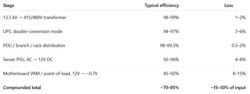
Traditional data centers receive power as high-voltage alternating current (HVAC, typically 13.8kV at the campus boundary), step it down through successive transformers to 480VAC, protect it through uninterruptible power supply (UPS) systems, distribute it through power distribution units (PDUs), rectify it to 12V direct current through server power supply units (PSUs), and finally step it down again through on-board voltage regulator modules (VRMs) to the 0.7-1.2V required by the processor die. This multi-stage cascade was engineered when a fully-loaded server rack drew 5-10kW. It delivers around 70-85% of grid electricity to the compute die, with the balance dissipated as heat in power conversion components and current paths. For a 1GW AI data center, even 85% power conversion efficiency means 150MW of power dissipated as heat during voltage conversion.
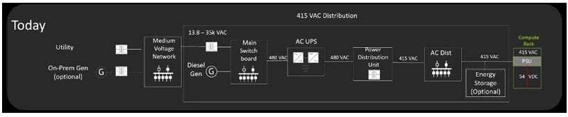
Source: Nvidia technical blog
While burning off 100,000+ homes worth of electricity every hour as heat would be immensely regrettable, the more fundamental physical constraint forcing the transition to 800VDC is current. A fundamental identity of electricity is Power equals Voltage times Current (P = V * I). At a fixed voltage (e.g. 48V), higher power requires proportionally higher current. This wasn’t an issue when server racks would draw 6-12kW of power, requiring up to 250A of current which could be handled by a copper wire the width of your pinky. At 140kW per rack, the GB300 NVL72 starts to really test the limits of the 48V rack architecture. By the time we get to the Rubin Ultra generation, a rack is expected to draw 600kW+ of power, which exceeds 12,500A of current at 48V. Based on Ohm’s Law Ploss = I2 * R, this 50x increase in current leads to a 2,500x increase in conduction loss assuming resistance R is constant. We would need a 2 meter long solid copper busbar with the cross-sectional area of an iPhone to deliver the required power to the GPUs.
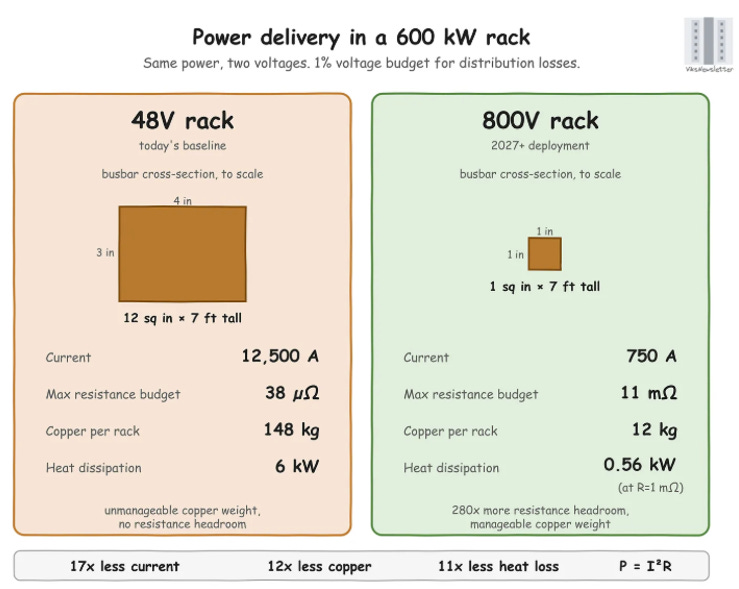
Source: Vik’s Newsletter
This is obviously not physically or economically viable at scale, so what is the solution? For a given power envelope, power loss scales quadratically with current and linearly with resistance. Halving the current by doubling the voltage reduces conduction loss by a factor of 4, while halving the resistance by doubling the cross-sectional area of the copper busbar only reduces conduction loss by half. Hence the industry’s solution has been to shift to 800VDC rack power architecture: this reduces rack current by 16.7x compared to 48V, which reduces conduction loss by 278x assuming resistance remains constant. Of course, resistance will increase as the size of the busbar shrinks from the area of an iPhone, but the overall net reduction in power loss will still be many multiples of the prevailing 48V architecture.
NVIDIA’s GPU thermal design power (TDP) trajectory is familiar to most technology investors, but its implications for power delivery infrastructure are less widely appreciated. The A100 at 400W was manageable within the 480V → 48V → 12V architecture. The H100 at 700W was manageable with upgraded cabling. The Blackwell GB200 NVL72 rack draws approximately 120kW across 72 GPUs and 36 CPUs. The forthcoming Vera Rubin and Rubin Ultra rack designs will ramp power consumption from 200kW to 600kW, and by the time the Feynman generation rolls around, single racks will draw over 1MW of power.
Two converging architecture standards
The industry has coalesced around higher DC bus voltages as the solution to the current density problem. Two standards have emerged in parallel. Mt. Diablo, backed initially by Microsoft and Meta and subsequently joined by Google, proposes ±400VDC (effectively 800V differential) delivered from standalone power cabinets to IT racks, published through the Open Compute Project. Its commercial deployments are expected from 2026. The standard retains the existing 480VAC backbone at the facility level and inserts a DC conversion shelf at the rack boundary. This is a more conservative approach that lowers adoption friction for hyperscalers with large existing AC infrastructure estates (which can be retrofitted), and leverages the established EV battery pack supply chain that has validated ~400V components at volume for over a decade.
Nvidia’s 800V HVDC architecture, unveiled at GTC 2025, is more radical: it replaces the 480VAC backbone entirely, delivering 800V monopolar DC from the utility interface throughout the data center floor and directly into racks. The architecture explicitly targets 1MW+ rack power densities consistent with Rubin Ultra and beyond. It is the more aggressive standard as it requires native 800VDC data center designs (existing LVAC data centers can’t be retrofitted), but also the one best suited to efficient high density power delivery as the industry converges on megawatt-scale racks.
The practical differences between the two standards matter less for the semiconductor content opportunity than their common element: both converge on roughly 800V delivered to the rack, and both require wide-bandgap power semiconductors at every conversion stage. However, the Mt. Diablo standard preserves more of the 480VAC architecture and thus incumbent power supply vendors, while Nvidia’s 800V reference design is more favorable to high-voltage, wide bandgap power semis suppliers.
The 800V power delivery chain: from grid to transistor
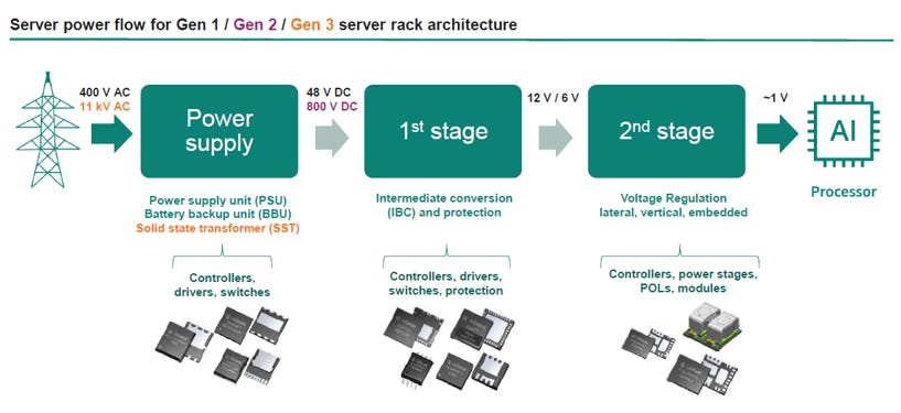
In the 800V HVDC architecture, power delivery from the utility interconnect to the compute die collapses from seven stages to three or four. A solid-state transformer (SST) converts 13.8kV AC directly to 800VDC at up to 99% efficiency, replacing the traditional multi-stage transformer-plus-UPS combination. An 800VDC bus runs throughout the data center floor: at 140kW per GB300 NVL72 rack, this requires only 175 amps which is manageable with a standard industrial bus bar and reportedly reduces copper requirements by approximately 45% versus an equivalent 54V architecture. A board-level HV DC-DC converter steps 800V to 12V (likely using SiC MOSFETs on the primary side and GaN on the secondary), achieving 97-98.5% efficiency at switching frequencies measured in hundreds of kilohertz. Finally, point-of-load VRMs adjacent to the GPU package step 6V or 12V down to the 0.7V core voltage required by the GPU.
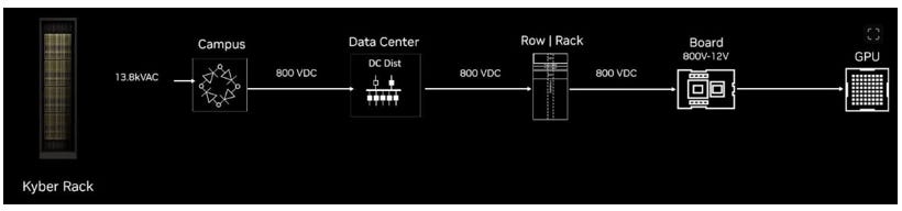
Source: Nvidia technical blog
The cumulative efficiency of this architecture can exceed 90%, against 70-85% for the legacy AC chain. For a 1GW data center, the improvement can avoid multiple tens of MWs in conversion losses compared to best-in-class 480VAC hyperscale architectures, which can then be used to power more compute (and as we know, compute = $$$).
For semiconductor companies, the shift to 800VDC changes the technical requirements at every stage of the power chain. Low-voltage silicon MOSFETs in simple buck topologies are supplanted by wide-bandgap devices – SiC for high-voltage switching, GaN for intermediate bus and POL – alongside isolated gate drivers, reinforced isolation components, and power management controllers. The bill of materials is richer and more technically demanding at every node, which is why companies with broad power portfolios like Infineon stand to capture disproportionate content per dollar of AI infrastructure spend.
The AI data center opportunity for Infineon
Infineon participates at virtually every stage of the AI data center power chain, which in our opinion makes the opportunity more interesting, albeit at the cost of maximum torque to any particular power stage. The company is present in the LV AC-DC (480VAC → 54/48VDC) and intermediate bus conversion (54/48V → 12/6V) stages through silicon MOSFETs and GaN devices used in PSU reference designs, and more critically, in the second stage VRM market through its OptiMOS TDM quad-phase modules that enable vertical power delivery. Management has most explicitly tied the AI revenue trajectory to the VRM and GaN stages, which is where Infineon’s technical differentiation is most defensible. Additionally, given Infineon’s strong position in SiC established over the years in the EV industry, we believe the company is also well positioned for the Solid State Transformer opportunity as that market develops towards the end of the decade.
Source: Infineon
Stage by stage
Source: Infineon
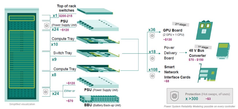
At the PSU stage (rack-level AC-to-DC conversion), Infineon supplies CoolMOS silicon power MOSFETs and GaN devices to PSU manufacturers including Delta, Murata, Bel, and Acbel. This is an indirect market where Infineon is designed in by the PSU maker rather than by the accelerator platform owner, and the silicon content at this stage is subject to competitive substitution at design-in cycles of 12-18 months. Texas Instruments, STMicroelectronics, onsemi, and Navitas amongst others compete with Infineon for PSU content. Content per unit is meaningful but not highly differentiated, so the value tends to be lower than for stages closer to the GPU itself.
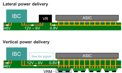
The intermediate bus conversion (IBC) stage is likely to see the most change during the transition to 800VDC architecture. The IBC stage itself basically exists as a compromise between distribution efficiency and POL feasibility as 54/48V is better for moving power across the server board (lower current), while 12/6V makes the final POL conversion down to ~0.7V easier. In the transitional 800V architecture, the 480VAC → 54/48VDC stage is replaced by an 800V → 54/48V DC-DC stage, with the LV IBC stage retained to preserve as much of the existing rack power infrastructure as possible to ease the transition. But the ultimate end state is to bring 800V straight into the server blade and perform a 67:1 conversion down to 12V near the GPU itself, thus minimizing the distance of the high-current low-voltage path. This would do away with the conventional LV IBC but require a much more demanding 800V → 12V high voltage isolated DC-DC converter.
We believe Infineon is well positioned for this shift because the HV DC-DC conversion stage moves the value pool towards the power semis components and module design where Infineon is strongest: high-voltage switching using a combination of Si, SiC and GaN, isolation, gate driving, sensing, protection, and system-level power control. The company forecasts the IBC SAM to grow at over 50% CAGR from 2025 to 2030, driven mainly by HV IBC, which supports our view that this stage will pull in a significant amount of high value power semis content from earlier stages.
In March 2026, the company introduced two HV IBC reference designs for 800V → 50V and 800V → 12V architectures using its CoolGaN switches. We understand that Infineon is currently the only company globally with scaled 300mm GaN wafer production versus the industry standard of 150mm or 200mm, which should enable materially lower die costs and tighter process control. This is not to say that Infineon will dominate this stage, as competitors like Texas Instruments and STMicro have both published their own 800V → 12V converter reference designs. But these kinds of major system-level transitions tend to reward vendors who can deliver a complete, integrated power semis portfolio.
Finally, the most strategically important stage is the second-stage voltage regulator module. These are the power modules that sit adjacent to or directly underneath the GPU package on the server board, converting the intermediate bus voltage to the GPU core voltage (typically 0.7-1V). This stage is technically demanding because it feeds voltage directly into the GPU power rails, must handle extremely high current (a 2,300W GPU package with 0.7V core voltage requires 3,300A of current), and is responsible for much of the power regulation required for the GPU’s very dynamic loads. Furthermore, as should be evident from the power delivery discussion above, this massive aggregate current at the chip level i) cannot be lowered unlike during earlier power stages, and ii) is where the largest efficiency losses occur. Therefore, VRM and power module vendors are increasingly turning to vertical power delivery (VPD) as a solution to the challenges presented by multi-kilowatt-rated AI processors.
Source: Infineon
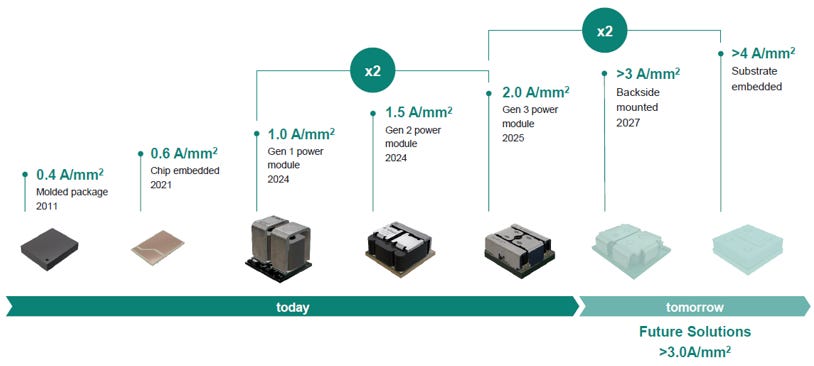
Infineon’s OptiMOS TDM2454xx quad-phase modules, announced in March 2025, deliver 2A per mm2 of current density and the company is working with Delta Electronics, the primary Nvidia power supply vendor, to enable VPD for AI processors. Management has committed to improving this to 3A/mm² by 2027, with substrate-integrated voltage regulation (SiVR) as the five-year horizon technology. By shortening the current path from centimeters as is the case with lateral power delivery where VRMs surround the GPU package, to millimeters through the compute board itself with VPD, conduction losses can be reduced by an order of magnitude (resistance scales linearly with the length of the conductor). Infineon also claims that its VPD modules enable higher power density, better thermals due to less power loss, and space savings on the compute board allowing for denser system designs.
Source: Infineon
The module business carries meaningfully higher gross margins than discrete MOSFETs because it integrates the gate driver, controller interface, and packaging in a form factor that reduces board space and design complexity for the customer, often supporting an ASP several times higher than the equivalent discrete component. Management has confirmed that AI power revenue is margin-accretive relative to the group’s high-teens segment result margin average. And on VPD specifically, management has also stated that these modules land at the high end of the power semis content range per installed kilowatt ($100-$250, more on this below).
“And for us, of course, the second stage part is giving us particular growth momentum. So we expect the share of the second stage in the overall numbers to increase over the quarters to come. As Andreas pointed out that vertical power deliveries, the modules have a much higher value. And again we are here teaming up with all GPU makers, or ASICS makers, whatever you want to call them (including in China).” – CEO, Q1 FY2026 analyst call
Sizing the AI data center opportunity
For paid subscribers, we discuss the size of Infineon’s AI power opportunity and the competitive landscape. Additionally, we dig into the positioning and outlook for the Automotive segment, the emerging AI-related opportunity within the Green Industrial Power segment, and consider whether an MCU shortage may emerge as the next opportunity for Infineon.